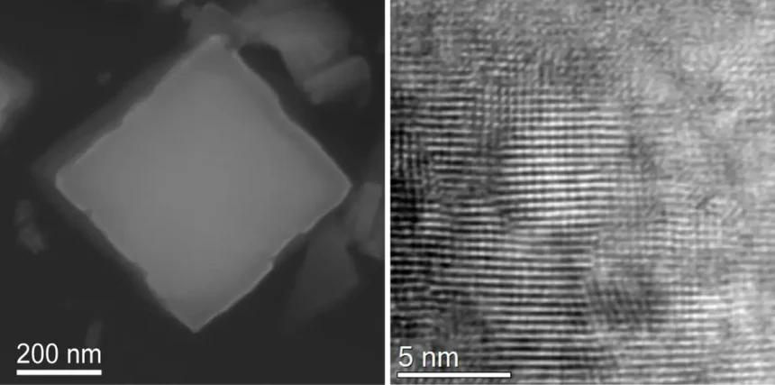

(Left) Single copper-doped tungstate nanocrystal. (Right) Atomic resolution image of nanocrystals.Credit: Melbert Ziem
Systematic copper doping improves tungsten’s total solar power utilization acid nanocrystal.
Sunlight is an inexhaustible energy source, and generating electricity using sunlight is one of the foundations of renewable energy. More than 40% of the sunlight that falls on Earth is in the infrared, visible and ultraviolet spectrum. However, current solar technology mainly uses visible and ultraviolet light. The technology for harnessing the entire spectrum of solar radiation, called total solar harvesting, is still in its infancy.
Hokkaido University research results
A team of researchers from Hokkaido UniversityA research group led by Associate Professor Melbert Ziem and Professor Seiichi Watanabe from the School of Engineering has synthesized a copper-doped tungstic acid-based material that exhibits all-solar utilization.Their findings were recently published in the journal advanced materials.
“Currently, the near-infrared and mid-infrared spectrum of solar radiation in the range of 800 nm to 2500 nm is not utilized for energy generation,” Jeem explains. “Tungstic acid has a defective crystal structure that absorbs these wavelengths, making it a candidate for developing nanomaterials that could potentially exploit this spectrum.”

A summary of the relative light absorption of tungstate crystals from ultraviolet to infrared light. 1, 5, and 10 are the copper concentrations that result in photocriticality of the nanocrystals. Credit: Melbert Jeem and other advanced materials. July 29, 2023
Methodology and results
The scientists synthesized tungstate nanocrystals doped with varying concentrations of copper using a previously developed photofabrication technique, microcrystal immersion photosynthesis. The structure and light absorption properties of these nanocrystals were analyzed. Their photothermal properties, photoassisted water evaporation properties, and photoelectrochemical properties were measured.
Copper-doped tungsten oxide nanocrystals absorb light across the spectrum from ultraviolet to visible to infrared. The amount of infrared radiation absorbed was highest at 1% copper doping. Nanocrystals doped with 1% and 5% copper showed the highest temperature rise (photothermal properties). The 1% copper-doped crystal also showed the highest water evaporation efficiency, approximately 1.0 kg/m2 per hour. Structural analysis of 1% copper-doped nanocrystals showed that copper ions may distort the crystal structure of tungsten oxide, resulting in the properties observed when light is absorbed.
conclusion
“Our findings represent an important advance in the design of nanocrystals that are capable of both synthesizing and harnessing total solar energy,” concludes Watanabe. “We have demonstrated through full solar applications that copper doping imparts different properties to tungstate nanocrystals. This provides a framework for further research and application development in this field. Offers.”
References: Melbert Ziehm, Ayaka Hayano, Hiroto Miyashita, Mahiro Nishimura, Kohei Fukuroi, Lin Xue-I, Lihua Zhang, and Seiichi Watanabe, “Tailored for full solar power generation use” “Defect-driven optical critical phase”, July 29, 2023, advanced materials.
DOI: 10.1002/adma.202305494
This research was supported by the Japan Society for the Promotion of Science (JSPS) Grant-in-Aid for Scientific Research (20H00295, 21K04823). Part of this research was made possible by the Hokkaido University Information Technology Center’s supercomputer system. This research was conducted at Hokkaido University with support from the Ministry of Education, Culture, Sports, Science and Technology’s Research Infrastructure for Advanced Materials and Nanotechnology (ARIM).